- Editors' Suggestion
- Access by Xinjiang University
Designing High-Efficiency Thin Silicon Solar Cells Using Parabolic-Pore Photonic Crystals
Phys. Rev. Applied 9, 044009 – Published 6 April, 2018
DOI: https://doi.org/10.1103/PhysRevApplied.9.044009
Abstract
We demonstrate the efficacy of wave-interference-based light trapping and carrier transport in parabolic-pore photonic-crystal, thin-crystalline silicon (-Si) solar cells to achieve above 29% power conversion efficiencies. Using a rigorous solution of Maxwell’s equations through a standard finite-difference time domain scheme, we optimize the design of the vertical-parabolic-pore photonic crystal (PhC) on a -thick -Si solar cell to obtain a maximum achievable photocurrent density (MAPD) of beyond the ray-optical, Lambertian light-trapping limit. For a slanted-parabolic-pore PhC that breaks symmetry, improved light trapping occurs due to better coupling into parallel-to-interface refraction modes. We achieve the optimum MAPD of for a tilt angle of 10° with respect to the vertical axis of the pores. This MAPD is further improved to by introducing a 75-nm antireflective coating on top of the solar cell. We use this MAPD and the associated charge-carrier generation profile as input for a numerical solution of Poisson’s equation coupled with semiconductor drift-diffusion equations using a Shockley-Read-Hall and Auger recombination model. Using experimentally achieved surface recombination velocities of , we identify semiconductor doping profiles that yield power conversion efficiencies over 29%. Practical considerations of additional upper-contact losses suggest efficiencies close to 28%. This improvement beyond the current world record is largely due to an open-circuit voltage approaching 0.8 V enabled by reduced bulk recombination in our thin silicon architecture while maintaining a high short-circuit current through wave-interference-based light trapping.
Physics Subject Headings (PhySH)
Article Text
References (61)
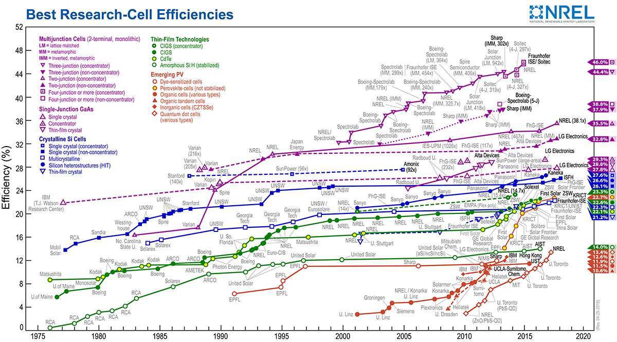
- National Renewable Energy Laboratory, Best research-cell efficiencies, https://www.nrel.gov/pv/assets/images/efficiency-chart.png (2016).
- W. Shockley and H. J. Queisser, Detailed balance limit of efficiency of junction solar cells, J. Appl. Phys. 32, 510 (1961).
- A. Richter, M. Hermle, and S. W. Glunz, Reassessment of the limiting efficiency for crystalline silicon solar cells, IEEE J. Photovoltaics 3, 1184 (2013).
- M. A. Green, K. Emery, Y. Hishikawa, W. Warta, E. D. Dunlop, D. H. Levi, and A. W. Y. Ho-Baillie, Solar cell efficiency tables (version 49), Prog. Photovoltaics 25, 3 (2017).
- K. Yoshikawa, H. Kawasaki, W. Yoshida, T. Irie, K. Konishi, K. Nakano, T. Uto, D. Adachi, M. Kanematsu, H. Uzu, and K. Yamamoto, Silicon heterojunction solar cell with interdigitated back contacts for a photoconversion efficiency over 26%, Nat. Energy 2, 17032 (2017).
- S. Hargreaves, L. E. Black, D. Yan, and A. Cuevas, Modelling of silicon solar cells with up-to-date material parameters, Energy Procedia 38, 66 (2013).
- S. Y. Herasimenka, W. J. Dauksher, and S. G. Bowden, open circuit voltage measured on thick silicon heterojunction solar cell, Appl. Phys. Lett. 103, 053511 (2013).
- S. Yoshiba, M. Hirai, Y. Abe, M. Konagai, and Y. Ichikawa, Single crystalline silicon solar cells with rib structure, AIP Adv. 7, 025104 (2017).
- S. John, Strong Localization of Photons in Certain Disordered Dielectric Superlattices, Phys. Rev. Lett. 58, 2486 (1987).
- E. Yablonovitch, Inhibited Spontaneous Emission in Solid-State Physics and Electronics, Phys. Rev. Lett. 58, 2059 (1987).
- G. Demsey and S. John, Solar energy trapping with modulated silicon nanowire photonic crystals, J. Appl. Phys. 112, 074326 (2012).
- S. Eyderman, S. John, and A. Deinega, Solar light trapping in slanted conical-pore photonic crystals: Beyond statistical ray trapping, J. Appl. Phys. 113, 154315 (2013).
- S. Eyderman, S. John, M. Hafez, S. S. Al-Ameer, T. S. Al-Harby, Y. Al-Hadeethi, and D. M. Bouwes, Light-trapping optimization in wet-etched silicon photonic crystal solar cells, J. Appl. Phys. 118, 023103 (2015).
- A. Chutinan and S. John, Light trapping and absorption optimization in certain thin-film photonic crystal architectures, Phys. Rev. A 78, 023825 (2008).
- T. Tiedje, E. Yablonovitch, G. Cody, and B. Brooks, Limiting efficiency of silicon solar cells, IEEE Trans. Electron Devices 31, 711 (1984).
- A. Mavrokefalos, S. E. Han, S. Yerci, M. S. Branham, and G. Chen, Efficient light trapping in inverted nanopyramid thin crystalline silicon membranes for solar cell applications, Nano Lett. 12, 2792 (2012).
- M. S. Branham, W. Hsu, S. Yerci, J. Loomis, S. V. Boriskina, B. R. Hoard, S. E. Han, and G. Chen, 15.7% efficient -thick crystalline silicon solar cells using periodic nanostructures, Adv. Mater. 27, 2182 (2015).
- S. Foster and S. John, Light-trapping design for thin-film silicon-perovskite tandem solar cells, J. Appl. Phys. 120, 103103 (2016).
- P. Kuang, S. Eyderman, M. L. Hsieh, A. Post, S. John, and S. Y. Lin, Achieving an accurate surface profile of a photonic crystal for near-unity solar absorption in a super thin-film architecture, ACS Nano 10, 6116 (2016).
- A. Luque and A. Marti, Increasing the Efficiency of Ideal Solar Cells by Photon Induced Transitions at Intermediate Levels, Phys. Rev. Lett. 78, 5014 (1997).
- R. W. Peng, M. Mazzer, and K. W. J. Barnham, Efficiency enhancement of ideal photovoltaic solar cells by photonic excitations in multi-intermediate band structures, Appl. Phys. Lett. 83, 770 (2003).
- K. Q. Le and S. John, Synergistic plasmonic and photonic crystal light-trapping: Architectures for optical upconversion in thin-film solar cells, Opt. Express 22, A1 (2014).
- A. Wang, J. Zhao, and M. A. Green, 24% efficient silicon solar cells, Appl. Phys. Lett. 57, 602 (1990).
- M. A. Green, K. Emery, Y. Hishikawa, and W. Warta, Solar cell efficiency tables (version 37), Prog. Photovoltaics 19, 84 (2011).
- S. J. Robinson, S. R. Wenham, P. P. Altermatt, A. G. Aberle, G. Heiser, and M. A. Green, Recombination rate saturation mechanisms at oxidized surfaces of high-efficiency silicon solar cells, J. Appl. Phys. 78, 4740 (1995).
- P. Mahtani, K. R. Leong, B. Jovet, D. Yeghikyan, and N. P. Kherani, High quality amorphous-crystalline silicon heterostructure prepared by grid-biased remote radio-frequency plasma enhanced chemical vapor deposition, J. Non-Cryst. Solids 358, 3396 (2012).
- B. Min, H. Wagner, A. Dastgheib-Shirazi, A. Kimmerle, H. Kurz, and P. P. Altermatt, Heavily doped Si:P emitters of crystalline Si solar cells: Recombination due to phosphorus precipitation, Phys. Status Solidi RRL 8, 680 (2014).
- R. S. Bonilla, B. Hoex, P. Hamer, and P. R. Wilshaw, Dielectric surface passivation for silicon solar cells: A review, Phys. Status Solidi A 214, 1700293 (2017).
- A. W. Blakers, Shading losses of solar-cell metal grids, J. Appl. Phys. 71, 5237 (1992).
- E. V. Kerschaver and G. Beaucarne, Back-contact solar cells: A review, Prog. Photovoltaics 14, 107 (2006).
- C. Battaglia, A. Cuevas, and S. D. Wolf, High-efficiency crystalline silicon solar cells: Status and perspectives, Energy Environ. Sci. 9, 1552 (2016).
- M. K. Mat Desa, S. Sapeai, A. W. Azhari, K. Sopian, M. Y. Sulaiman, N. Amin, and S. H. Zaidi, Silicon back contact solar cell configuration: A pathway towards higher efficiency, Renewable Sustainable Energy Rev. 60, 1516 (2016).
- S. Bhattacharya and S. John (to be published).
- M. F. Schumann, S. Wiesendanger, J. C. Goldschmidt, B. Blasi, K. Bittkau, U. W. Paetzold, A. Sprafke, R. B. Wehrspohn, C. Rockstuhl, and M. Wegner, Cloaked contact grids on solar cells by coordinate transformations: Designs and prototypes, Optica 2, 850 (2015).
- M. Langenhorst, M. F. Schumann, R. Schmager, J. Lehr, U. Lemmer, M. Wegener, B. Richards, and U. W. Paetzold, in Proceedings of Optical Nanostructures and Advanced Materials for Photovoltaics, Boulder, 2017 (Optical Society of America, Washington, DC, 2017), p. PW2A.3.
- M. F. Schumann, M. Langenhorst, M. Smeets, K. Ding, U. W. Paetzold, and M. Wegener, All-angle invisibility cloaking of contact fingers on solar cells by refractive free-form surfaces, Adv. Opt. Mater. 5, 1700164 (2017).
- E. S. Roman, A. Vitrey, J. Buencuerpo, I. Prieto, J. M. Llorens, A. Garcia-Martin, B. Alen, A. Chaudhuri, A. Neumann, S. R. J. Brueck, and J. M. Ripalda, Cloaking of solar cell contacts at the onset of Rayleigh scattering, Sci. Rep. 6, 28669 (2016).
- Z. R. Chowdhury, K. Cho, and N. P. Kherani, High-quality surface passivation of silicon using native oxide and silicon nitride layers, Appl. Phys. Lett. 101, 021601 (2012).
- S. Calnan, O. Gabriel, I. Rothert, M. Werth, S. Ring, B. Stannowski, and R. Schlatmann, Influence of chemical composition and structure in silicon dielectric materials on passivation of thin crystalline silicon on glass, ACS Appl. Mater. Interfaces 7, 19282 (2015).
- I. Valuev, A. Deinega, A. Knizhnik, and B. Potapkin, in Computational Science and Its Applications—ICCSA 2007, edited by O. Gervasi and M. L. Gavrilova, Lecture Notes in Computer Science, Vol. 4707 (Springer, New York, 2007), p. 213.
- A. Deinega and S. John, Finite difference discretization of semiconductor drift-diffusion equations for nanowire solar cells, Comput. Phys. Commun. 183, 2128 (2012).
- M. A. Green, Self-consistent optical parameters of intrinsic silicon at 300 K including temperature coefficients, Sol. Energy Mater. Sol. Cells 92, 1305 (2008).
- G. Masetti, M. Severi, and S. Solmi, Modeling of carrier mobility against carrier concentration in arsenic-, phosphorus-, and boron-doped silicon, IEEE Trans. Electron Devices 30, 764 (1983).
- B. J. Hallam, P. G. Hamer, S. R. Wenham, M. D. Abbott, A. Sugianto, A. M. Wenham, C. E. Chan, G. Q. Xu, J. Kraiem, J. Degoulange, and R. Einhaus, Advanced bulk defect passivation for silicon solar cells, IEEE J. Photovoltaics 4, 88 (2014).
- A. Richter, S. W. Glunz, F. Werner, J. Schmidt, and A. Cuevas, Improved quantitative description of Auger recombination in crystalline silicon, Phys. Rev. B 86, 165202 (2012).
- T. Luder, G. Hahn, and B. Terheiden, Passivation of Si wafers by ALD- films with different surface conditioning, Energy Procedia 8, 660 (2011).
- J. Benick, A. Richter, M. Hermle, and S. W. Glunz, Thermal stability of the passivation on -type silicon surfaces for solar cell applications, Phys. Status Solidi RRL 3, 233 (2009).
- M. J. Kerr and A. Cuevas, General parameterization of Auger recombination in crystalline silicon, J. Appl. Phys. 91, 2473 (2002).
- A. Luque and I. Tobias, Perimeter recombination in planar solar cells, J. Appl. Phys. 73, 4042 (1993).
- Synopsys, tcad sentaurus, release M-2016.12, 2016.
- H. Cui, P. R. Campbell, and M. A. Green, Optimisation of the back surface reflector for textured polycrystalline Si thin film solar cells, Energy Procedia 33, 118 (2013).
- S. Eyderman, A. Deinega, and S. John, Near perfect solar absorption in ultra-thin-film GaAs photonic crystals, J. Mater. Chem. A 2, 761 (2014).
- Z. C. Holman, M. Filipic, B. Lipovsek, S. De Wolf, F. Smole, M. Topic, and C. Ballif, Parasitic absorption in the rear reflector of a silicon solar cell: Simulation and measurement of the sub-bandgap reflectance for common dielectric/metal reflectors, Sol. Energy Mater. Sol. Cells 120, 426 (2014).
- P. B. Johnson and R. W. Christy, Optical constants of the noble metals, Phys. Rev. B 6, 4370 (1972).
- A. Vial, T. Laroche, M. Dridi, and L. L. Cunff, A new model of dispersion for metals leading to a more accurate modeling of plasmonic structures using the FDTD method, Appl. Phys. A 103, 849 (2011).
- See http://www.pveducation.org/pvcdrom/design/emitter-resistance.
- F. Feldmann, M. Bivour, C. Reichel, M. Hermle, and S. W. Glunz, Passivated rear contacts for high-efficiency -type Si solar cells providing high interface passivation quality and excellent transport characteristics, Sol. Energy Mater. Sol. Cells 120, 270 (2014).
- PV Lighthouse, Sheet-resistance calculator, https://www2.pvlighthouse.com.au/calculators/Sheet%20resistance%20calculator/Sheet%20resistance%20calculator.aspx.
- M. J. Kerr, J. Schmidt, A. Cuevas, and J. H. Bultman, Surface recombination velocity of phosphorus-diffused silicon solar cell emitters passivated with plasma enhanced chemical vapor deposited silicon nitride and thermal silicon oxide, J. Appl. Phys. 89, 3821 (2001).
- M. Muller et al., Loss analysis of 22% efficient industrial PERC solar cells, Energy Procedia 124, 131 (2017).
- A. Schenk, Finite-temperature full random-phase approximation model of band gap narrowing for silicon device simulation, J. Appl. Phys. 84, 3684 (1998).